MSP - Wafer Contamination Standards
Characterize and optimize the sensitivity and overall performance of your wafer inspection system with Wafer Contamination Standards from MSP. These high-quality wafer inspection standards are made to your specifications with a quick turn-around, enabling short learning cycles during tool development and providing timely quality assurance for installed systems.
MSP Wafer Contamination Standards consist of particles deposited on a wafer (100 mm to 450 mm) with the industry's best particle size and count control. Using the advanced particle generation and DMA technology of MSP's Particle Deposition Systems, the modal diameter of deposited nanoparticles is controlled with nanometer-level accuracy and sub-nanometer resolution.Triple wrapped wafer packaging
Every substrate is handled with extreme care and packaged with MSP's signature triple-wrap packaging, preventing contamination during transport.
Deposit Patterns:
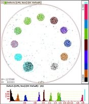
Particles can be deposited in Spot, Full (Blanket), Arc, and Ring patterns.
Particle Materials/Types:
Particle size standards available for deposition include spheres of PSL (polystyrene latex) and SiO2 (including MSP NanoSilica™ Size Standards). MSP Process Particles™ Suspensions are offered in 13 materials for deposition.
Wafer Contamination Standard Base Items:
The Wafer Contamination Standard includes a base item, which consists of one deposit on a wafer. MSP provides 150 mm, 200 mm, and 300 mm bare silicon (Si) wafers. Customers can also provide wafers of their choice (bare, film, patterned) for deposition, including wafers constructed from materials other than silicon (e.g., glass). Wafers as small as 100 mm and as large as 450 mm can be processed.
The base item includes a Deposition Summary, Certificate of Conformance, Certificate of Calibration for each particle size standard, and triple-wrap packaging.
Features & Benefits
•Widest range of particle materials and sizes
•Over 100 particle size standards available
•Customizable deposit patterns and locations
•Particle size control with nanometer-level accuracy for nanoparticles
•Consistent particle size with sub-nanometer resolution for nanoparticles
•Particle count from 100 to millions per recipe
•Quick turnaround for faster learning
•Triple-wrap packaging for low-adder transport
Applications
•Wafer inspection tool calibration
•Inspection tool development and qualification
•Incoming wafer inspection/qualification
•Production wafer monitoring
Download Datasheet
Direct Contact


